- 您现在的位置:买卖IC网 > Sheet目录255 > T3V3LCS3-7 (Diodes Inc)TVS UNIDIRECT 350W 3.3V SOD-323
NOT RECOMMENDED FOR NEW DESIGNS
T3V3LCS3
LOW CAPACITANCE SURFACE MOUNT TVS
Features
Mechanical Data
?
?
?
?
?
?
?
?
350 Watts Peak Pulse Power (tp = 8x20 μ s)
IEC 61000-4-2 (ESD): Air – 15kV, Contact – 8kV
IEC 61000-4-4 (EFT): 40A – 5/50ns
IEC 61000-4-5 (Surge): 24A, 8/20 μ s – Level 2(Line-Gnd) & Level
3(Line-Line)
Low Capacitance, typ. = 3 pF
Unidirectional Configuration
Lead Free/RoHS Compliant (Note 4)
“Green” Device (Note 5)
?
?
?
?
?
?
?
?
1
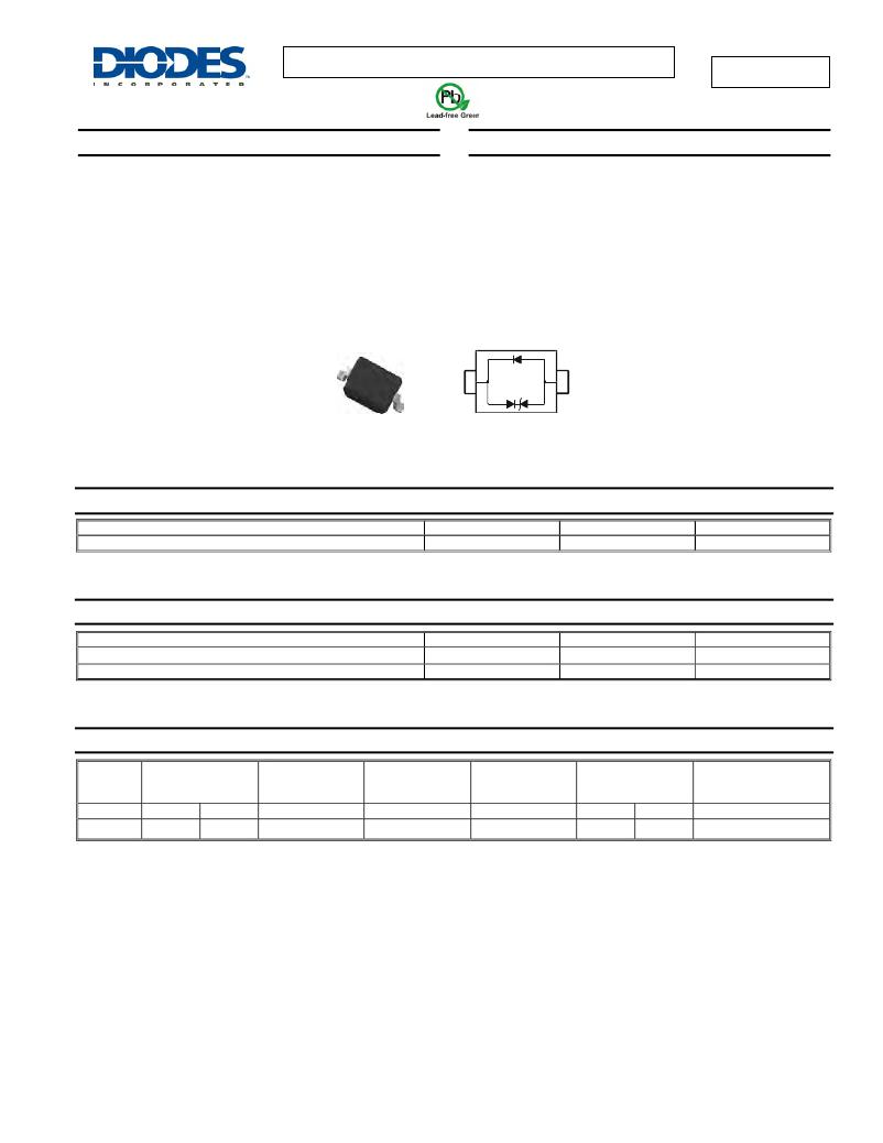
Case: SOD-323
Case Material: Molded Plastic, “Green” Molding Compound,
Note 5. UL Flammability Classification Rating 94V-0
Moisture Sensitivity: Level 1 per J-STD-020
Terminals: Matte Tin Finish annealed over Alloy 42 leadframe
(Lead Free Plating). Solderable per MIL-STD-202, Method 208
Polarity: Cathode Band, See Page 2
Marking Information: See Page 2
Ordering Information: See Page 2
Weight: 0.004 grams (approximate)
2
TOP VIEW
Top View
Device Schematic
Maximum Ratings
@T A = 25°C unless otherwise specified
Characteristic
Peak Pulse Power (tp = 8x20 μ s) (Note 7) T A = 25°C
Symbol
P pk
Value
350
Unit
W
Thermal Characteristics
Characteristic
Thermal Resistance, Junction to Ambient (Note 7) T A = 25°C
Operating and Storage Temperature Range
Symbol
R θ JA
T J , T STG
Value
425
-55 to +150
Unit
° C/W
° C
Electrical Characteristics
@T A = 25°C unless otherwise specified (Note 8)
Reverse
Standoff
Voltage
Breakdown Voltage
V BR @ I T
Test
Current
Max. Reverse Max. Clamping
Leakage @ V RWM Voltage @ I pp = 1A
(Note 6) (Note 3)
Max. Clamping
Voltage V C @ I PP
(Note 3)
Typical Total
Capacitance C T
(Note 1)
V RWM (V)
3.3
Min (V)
4.0
Max (V)
?
I T (mA)
1.0
I R ( μ A) V C (V)
5 7
V C (V) I PP (A)
19 20
(pF)
3
Notes:
1.
2.
3.
4.
5.
6.
7.
8.
V R = 0V, f = 1MHz.
tp = 8x20 μ s.
Clamping voltage value is based on an 8x20 μ s peak pulse current (I pp ) waveform (see figure 1).
No purposefully added lead.
Diodes Inc.’s “Green” policy can be found on our website at http://www.diodes.com/products/lead_free/index.php.
Short duration pulse test used to minimize self-heating effect.
Device mounted on FR-4 PC board with suggested pad layout, which can be found on page 3 or on our website at
Positive potential is applied from pin 1 to pin 2.
T3V3LCS3
Document number: DS31104 Rev. 7 - 3
1 of 4
November 2009
? Diodes Incorporated
发布紧急采购,3分钟左右您将得到回复。
相关PDF资料
T491X107K025AT
CAP TANT 100UF 25V 10% 2917
T521D107M016ATE050
CAP TANT 100UF 16V 20% 2917
T525D337M006ATE040
CAP TANT 330UF 6.3V 20% 2917
T620162004DN
SCR PHASE CTRL MOD 1600V 200A
T68-1/M
TERMINAL MINIWRAP .042" GOLD
T6V0S5-7
TVS 260W 6.0V SOD-523
T720224504DN
SCR PHASE CTRL MOD 2200V 450A
T7H8146504DN
SCR PHASE CTRL MOD 1400V 650A
相关代理商/技术参数
T3V3S5
制造商:DIODES 制造商全称:Diodes Incorporated 功能描述:UNIDIRECTIONAL SURFACE MOUNT TVS
T3V3S5-7
功能描述:TVS 二极管 - 瞬态电压抑制器 150MW 3.3V RoHS:否 制造商:Vishay Semiconductors 极性:Bidirectional 工作电压: 击穿电压:58.9 V 钳位电压:77.4 V 峰值浪涌电流:38.8 A 系列: 封装 / 箱体:DO-214AB 最小工作温度:- 55 C 最大工作温度:+ 150 C
T3W
制造商:SPC Multicomp 功能描述:BOX ABS WHITE 制造商:SPC Multicomp 功能描述:BOX, ABS, WHITE 制造商:SPC Multicomp 功能描述:ENCLOSURE, WALL MOUNT, PLASTIC, WHITE, Enclosure Type:Box, Enclosure Material:ABS, Body Color:White, External Height - Imperial:1.06", External Height - Metric:27mm, External Width - Imperial:2.95", External Width - Metric:75mm , RoHS Compliant: Yes
T3W-1215-10W-133
制造商:Amphenol Corporation 功能描述:E38999/SHELL - Bulk
T3W-1215-20W-133
制造商:Amphenol Corporation 功能描述:E38999/SHELL - Bulk
T3W-1215-25SN
制造商:Amphenol Corporation 功能描述:MIL-C-38999 SERIES III SCOOP PROOF THREADED - Bulk 制造商:Amphenol Corporation 功能描述:T3 25C 22#22S 3#16 SKT PLUG
T3W-1217-20PA
制造商:Amphenol Corporation 功能描述:MIL-C-38999 SERIES III SCOOP PROOF THREADED - Bulk
T3W-1217-20PA-105
制造商:Amphenol Corporation 功能描述:MIL-C-38999 SERIES III SCOOP PROOF THREADED - Bulk
